Vámi zadanému slovu odpovídají následující pojmy či výrazy:
Nenašli jste co jste hledali? Kontaktujte nás na adrese issn@gate2biotech.com
p-n junction

A p–n junction is formed at the boundary between a p-type and n-type semiconductor created in a single crystal of semiconductor by doping. If two separate pieces of material were used, this would introduce a grain boundary between the semiconductors that severely inhibits its utility by scattering the electrons and holes.
p–n junctions are elementary "building blocks" of most semiconductor electronic devices such as diodes, transistors, solar cells, LEDs, and integrated circuits; they are the active sites where the electronic action of the device takes place. For example, a common type of transistor, the bipolar junction transistor, consists of two p–n junctions in series, in the form n–p–n or p–n–p.
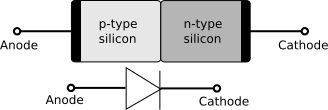
Silicon p-n junction.
Vnější zdroje: